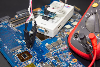
Bios Working secuence
Before press Power Button
When Ec Provided by power it active the analog and digital
power Section

By default it generate clock on clock pins (32.768 khz). If
Susclk is used then it provided
by Intel chipset by rtc section activity.

When Clock is on Clock then Ec reset is take place. This
delay must be take place after
clock generation. That is because use of RC circuit used on
ECRST#.

After ECRST# EC
output clock on EC Bios pin no.6 that is usually 12mhz to 30mhz you
can check it by removing bios chip and than check pin6 for
clock with DSO. This is the
signal which make bios active to input and output data and
time selection for chip select
signal to read write operation.
When bios is mounted 3.3v must be there on pin8, pin7and
pin3
Pin 8 is for vcc power for bios chip. Pin 7 for hold for
pause operations when use low
buffer area. Pin 3 is for write protection for device.

When clock present on pin6. EC control CS# signal for Data
input and output operations
When CS# is High chip is not select for Data input and
output when CS# is in low then
EC Input and output made. Ec input data for certain address
to read from pin5 and output
Will make from pin2 . Data is generally used in 8 bit.


Comments
Post a Comment